1. System Overview
▫️ Design Goals
- Implement automatic switching between dual power inputs (Type-C/Battery), 5V (Type-C)/4.2V (Battery).
- Implement power on/off through long press of button using EC190708.
- Integrate Ai-M61-32S Wi-Fi 6/BLE module for wireless communication.
- Implement offline voice wake-up and interruption through VB6824 offline voice chip, supporting audio capture, playback, and ACE echo cancellation.
▫️ Overall Architecture Diagram
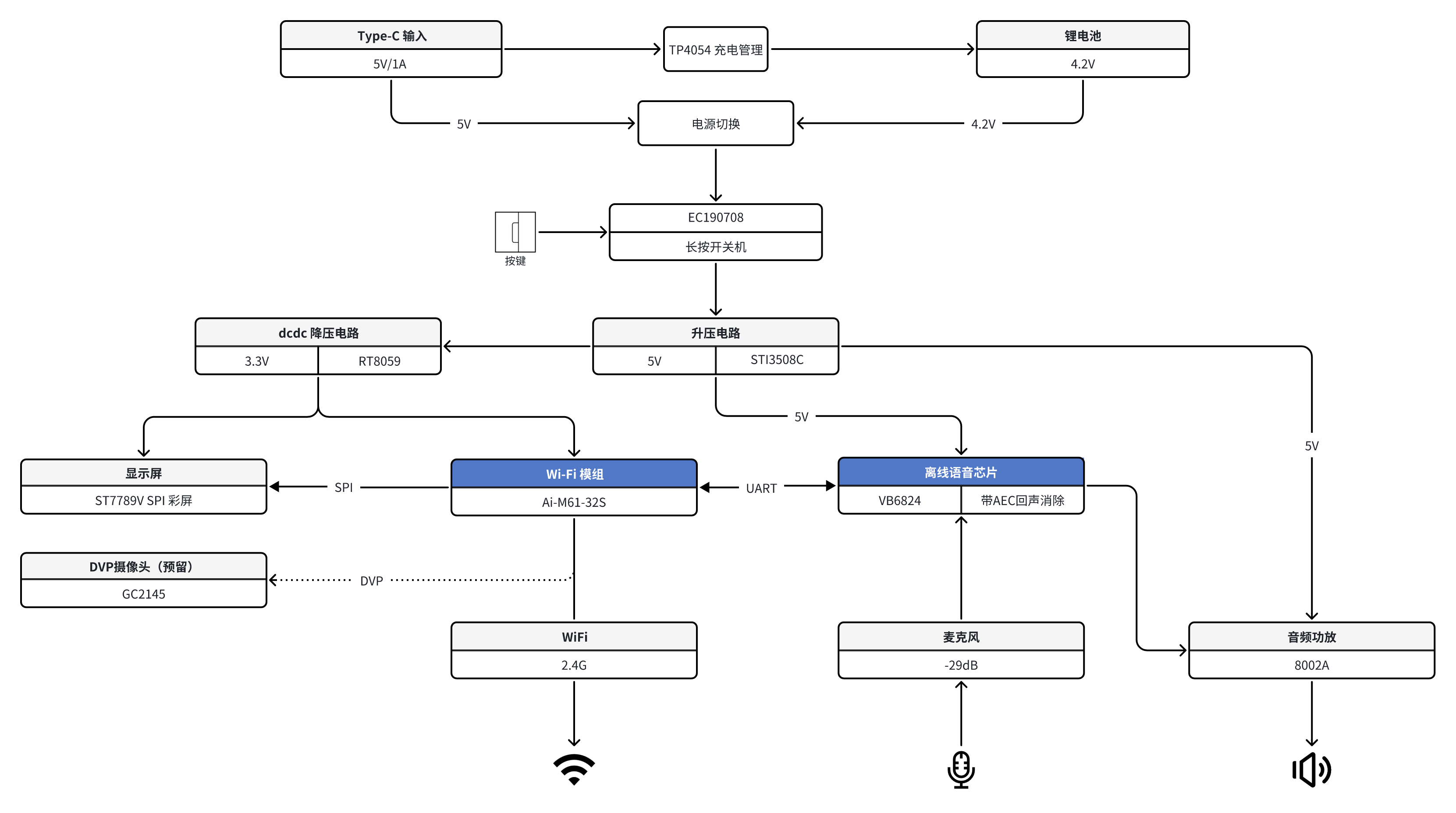
2. Module Design Specifications
▫️ Power Module
🔹 Function Description
- Dual power input: Automatic switching between Type-C (5V) and lithium battery (3.7V), with priority given to Type-C power supply;
- Charging management: TP4054 implements constant current/constant voltage charging for lithium battery, with maximum charging current of 500mA;
- Boost output: When powered by battery, outputs 5V system voltage through boost chip (such as STI3508C);
- Buck output: Steps down 5V to 3.3V to power modules and voice chips.
🔹 Design Points
- TP4054 key parameters:
- Charging current setting:
(e.g., R=5kΩ → 200mA), can also refer to the table below for configuration.
- Charging current setting:
| 5.1 | 200 |
| 4.7 | 250 |
| 4.3 | 300 |
| 4.0 | 400 |
| 3.7 | 500 |
| 3.4 | 600 |
| 3.1 | 667 |
| 2.8 | 800 |
| 2.5 | 1000 |
| 2.2 | 1200 |
- BAT pin requires a ceramic capacitor of 10μF or more;
- Boost circuit design:
- Boost IC model used: STI3508C;
- Feedback resistor calculation:
, where =0.6V. (e.g., R1=110kΩ, R2=15kΩ → 5.00V); - Inductor selection: 2.2μH recommended.
(Click to view) Reference circuit:
- Recommended selection table for common voltages:
| R1 (KΩ) | R2(KΩ) | C2 (uF) | L(uH) | |
|---|---|---|---|---|
| 5 | 110 | 15 | 22 | 2.2~6.8 |
| 9 | 130 | 9.31 | 22 | 4.7~10 |
| 10 | 24 | 200 | 5.11 | 22 |
- Buck circuit:
⁉️Why are both boost and buck circuits needed?
A: The purpose of the boost is to ensure a stable power supply for the power amplifier chip when powered by the battery, maintaining consistent audio quality. The buck circuit is mainly used to power the WiFi module and audio chips.
- DC/DC chip signal: RT8059;
- Feedback resistor calculation:
, where =0.6V, for example (R1=68KΩ, R2=15KΩ → 3.32V);
(Click to view) Reference circuit:
- Power switching logic:
- When Type-C is inserted, cut off the battery power supply path through MOSFET (such as AO3401).
🔹 Interface Definition
| Pin/Net Name | Type | Description |
|---|---|---|
| USB_5V | Input | Type-C 5V Power Input |
| BAT+ | Input/Output | Lithium battery positive terminal (3.7V) |
| VCC_5V | Output | System main power supply (5V±5%) |
| VCC_3V3 | Output | Power supply for modules and voice chips (3.3V ±5%) |
🔹 Layout Recommendations
- Thermal management: TP4054 and boost chip should be kept away from sensitive analog circuits, with adequate copper coverage on ground heat dissipation pads;
- Decoupling capacitors: Parallel 10μF electrolytic capacitor + 0.1μF ceramic capacitor at VCC_5V and VCC_3V3 output terminals.
▫️ AiM6132S Module
🔹 Function Description
- Provides Wi-Fi/BLE dual-mode wireless connection, communicates with main controller through UART;
- Operating voltage: 3.3V@500mA peak.
🔹 Design Points
- Power design:
- Recommended DC/DC chip: RT8059, input needs to be ≥4V, output 3.3V;
- Decoupling capacitors: 10μF+0.1μF close to the module VCC pin.
- UART interface:
- LOG:
- Interface: RX0 (RX) & TX0 (TX);
- Default baud rate: 2000000.
- Offline voice communication port:
- Interface: IO19 (RX) & IO18 (TX);
- Default baud rate: 2000000.
- LOG:
- Antenna layout:
- Copper covering is prohibited in the PCB antenna area, with a clearance area of ≥5mm around.
- Module interface definition:
| Pin Number | Pin Name | Description |
|---|---|---|
| 1 | GND | Power ground |
| 2 | VDD33 | 3v3 power supply |
| 3 | CHIP_EN | Module reset pin |
| 4 | GPIO0 | Reserved I2C pin: I2C_SCL |
| 5 | GPIO1 | Reserved I2C pin: I2C_SDA |
| 6 | GPIO16 | SPI screen RS pin |
| 7 | GPIO17 | DCX_SPI_SCL |
| 8 | GPIO12 | CSX_SPI_CS |
| 9 | GPIO14 | NC |
| 10 | GPIO15 | SPI_MOSI |
| 11 | GPIO18 | UART TX signal of offline voice chip |
| 12 | GPIO19 | UART RX signal of offline voice chip |
| 13 | GPIO10 | Led out GPIO10 |
| 14 | GPIO13 | Led out GPIO13 |
| 15 | GPIO11 | NC |
| 16 | GPIO3 | DVP_RSTB |
| 17 | GPIO20 | AI_LCD |
| 18 | GPIO4 | External Flash, not available |
| 19 | GPIO5 | External Flash, not available |
| 20 | GPIO6 | External Flash, not available |
| 21 | GPIO7 | External Flash, not available |
| 22 | GPIO8 | External Flash, not available |
| 23 | GPIO9 | External Flash, not available |
| 24 | USB_DP | USB_DP |
| 25 | USB_DM | USB_DM |
| 26 | GPIO23 | DVP_MCLK |
| 27 | GPIO2 | Boot control pin, high level at power-on enters programming mode |
| 28 | GPIO24 | DVP_D0 |
| 29 | GPIO28 | DVP_HYSNC |
| 30 | GPIO26 | DVP_D2 |
| 31 | GPIO25 | DVP_D1 |
| 32 | GPIO27 | DVP_D3 |
| 33 | GPIO29 | DVP_VSYNC |
| 34 | GPIO30 | DVP_CLK |
| 35 | GPIO31 | DVP_D4 |
| 36 | TX0 | UART_TX |
| 37 | RX0 | UART_RX |
| 38 | GPIO32 | DVP_D5 |
| 39 | GPIO33 | DVP_D6 |
| 40 | GPIO34 | DVP_D7 |
▫️ SPI Color Screen Driver Circuit
- The selected screen supports 5V power supply, uses IO2 to control the backlight, and realizes software control of brightness
- Pin header design, the screen is connected to the baseboard in the form of pin headers
▫️ Offline Voice Module (VB6824+8002A)
🔹 Function Description
- VB6824 implements voice wake-up word recognition and audio encoding/decoding, interacts with Ai-M61-32S through UART;
- 8002A power amplifier drives 8Ω/2W speaker, supports PWM input.
🔹 Design Points
- Audio circuit:
- A 100nF DC blocking capacitor is connected in series between VB6824 and 8002A;
- Speaker traces need to be thickened (≥0.5mm) to avoid being parallel to digital signal lines.
- Microphone design:
- It is recommended to use an omnidirectional cylindrical omnidirectional microphone with a sensitivity of -29dB ±3dB;
- Microphone power supply requires RC filtering (4.7KΩ+10uF).
- AEC echo cancellation:
- The speaker output pin (DACR) is connected in series with a 0.1uF capacitor and a 5.1KΩ resistor to PA1 and PA0;
(Click to view) Reference circuit:
- Power amplifier configuration:
- 8002A gain setting: Avd= 2×(Rf/Ri) (default Rf=30K, Ri=10K, gain 6 times).
- VB6824 main interface definition:
| Pin Number | Pin Name | Description |
|---|---|---|
| 1 | USBDM | Programming and LOG pin |
| 2 | USBDP | Programming and LOG pin |
| 3 | PA1 | AEC echo cancellation acquisition pin |
| 4 | PA0 | AEC echo cancellation acquisition pin |
| 5 | PC7/MIC_BIAS | Microphone driver pin |
| 6 | MIC | MIC input interface |
| 11 | DACR | Audio signal output pin, output to audio power amplifier chip |
| 14 | PB10 | RX signal of communication UART |
| 15 | PB9 | TX signal of communication UART |
| 17 | PB5 | Power amplifier control signal |
3. Debugging and Testing
▫️ Power Test Items
| Test Point | Expected Value | Allowable Error |
|---|---|---|
| TP4054 PROG | 0.5V (500mA) | ±5% |
| VCC_5V | 5.0V | ±3% |
| DC/DC Output | 3.3V | ±2% |
▫️ Voice Module Verification
- Wake-up test: At a distance of 30cm, when the signal-to-noise ratio is ≥15dB, the wake-up rate is >95%;
- Audio distortion: THD of 1kHz sine wave output <1%.