Ra-01/Ra-02 LoRa Module User Manual
Ra-01/Ra-02 LoRa Module User Manual
Disclaimer and copyright notice
The information in this article, including the URL address for reference, is subject to change without notice. To
The document is provided “as is” and does not bear any guarantee responsibility, including any guarantee for marketability, suitability for a specific purpose, or non-infringement, and any guarantee mentioned elsewhere in any proposal, specification or sample. This document does not take any responsibility, including the responsibility for infringement of any patent rights caused by using the information in this document. This document does not grant any permission to use intellectual property rights in estoppel or other ways, whether express permission or implied permission. To
All brand names, trademarks and registered trademarks mentioned in this article are the property of their respective owners, and it is hereby declared. To
Notes
Due to product version upgrades or other reasons, the contents of this manual may change. Shenzhen Anxinke Technology Co., Ltd. reserves the right to modify the contents of this manual without any notice or prompt. This manual is only used as a guide. Shenzhen Anxinke Technology Co., Ltd. makes every effort to provide accurate information in this manual. However, Shenzhen Anxinke Technology Co., Ltd. does not guarantee that the contents of the manual are completely free of errors. All statements and information in this manual And suggestions do not constitute any express or implied guarantee.
1. Overview
Anxinke LoRa series modules (Ra-01/Ra-02) are designed and developed by Anxinke Technology. The radio frequency chip of this series of modules SX1278 mainly uses LoRa™ remote modem for ultra-long-distance spread spectrum communication. It has strong anti-interference and can Minimize current consumption. With the help of SEMTECH's LoRa™ patented modulation technology, SX1278 has a high sensitivity of over -148dBm, a power output of +20dBm, a long transmission distance and high reliability. At the same time, compared with traditional modulation technology, LoRa™ modulation technology also has obvious advantages in anti-blocking and selection, which solves the problem of distance, anti-interference and power consumption that traditional design solutions cannot simultaneously take into account.
Figure 1 Functional block diagram of SX1278
1.1 Ra-01/Ra-02 module characteristics
• LoRa™ modem
• Support FSK, GFSK, MSK, GMSK, LoRa™ and OOK modulation methods
• Support frequency band 410MHz~525MHz
• The working voltage is 3.3V, the maximum output is +20dBm, and the maximum working current is 105mA
• It has low power consumption characteristics in the receiving state, the receiving current is 12.15mA, the standby current is 1.6mA
• High sensitivity: as low as -140dBm
• Small size double row stamp hole patch package
• The module adopts SPI interface, half-duplex communication, with CRC, up to 256-byte packet engine
1.2 Main parameters of Ra-01/Ra-02 module
Table 1 Ra-01/Ra-02 module parameter table
| Category | Parameters | Description |
| Package | SMD-16 | |
| Size | 17*16*3.2(±0.2)mm | |
| Frequency range | 410~525MHz | |
| Communication interface | SPI | |
| Programmable bit rate | Up to 300Kbps | |
| Maximum transmit power | 20±1 dBi | |
| Working voltage | 2.7~3.6V, typical value 3.3V | |
| Working temperature | -20~+70°C | |
| Storage environment | -40~+125°C,<90%RH | |
| Weight | 0.45g |
1.3 Recommended working environment
| Working environment | Name | Minimum value | Typical value | Maximum value | Unit |
| Supply voltage | VDD | 2.7 | 3.3 | 3.6 | V |
| Working temperature | TOPR | -20 | 25 | 70 | ℃ |
| IO level | VIO | 2.7 | 3.3 | 3.6 | V |
| Digital input low level | VIL | - | - | 0.2 | V |
| Digital input high level | VIH | 0.8 | - | - | V |
| Digital output low level | VoL | - | - | 0.1 | V |
| Digital output high level | VoH | 0.9 | - | - | V |
1.4 Application
- Automatic meter reading
- Smart home and security system
- Industrial monitoring and control
- Home and building automation
- Remote irrigation system
- Wireless sensor data collection
2 Interface definition
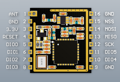
2.1 Ra-01/Ra-02 module pin diagram
2.2 Ra-01/Ra-02 module pin function definition
| Pin number | Pin name | Function description | |
| Ra-01 | Ra-02 | ||
| 1 | - | ANT | Antenna |
| 2 | 1, 2 | GND | Ground |
| 3 | 3 | 3.3V | 3.3V power supply |
| 4 | 4 | RESET | Reset |
| 5 | 5 | DIO0 | Digital IO0, software configuration |
| 6 | 6 | DIO1 | Digital IO1 software configuration |
| 7 | 7 | DIO2 | Digital IO2 software configuration |
| 8 | 8 | DIO3 | Digital IO3 software configuration |
| 9 | 9 | GND | Ground |
| 10 | 10 | DIO4 | Digital IO 4-piece configuration |
| 11 | 11 | DIO5 | Digital IO5 software configuration |
| 12 | 12 | SCK | SPI clock input |
| 13 | 13 | MISO | SPI data output |
| 14 | 14 | MOSI | SPI data input |
| 15 | 15 | NSS | SPI chip select input |
| 16 | 16 | GND | Ground |
3 Ra-01/Ra-02 module package size drawing
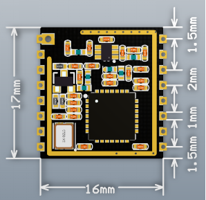
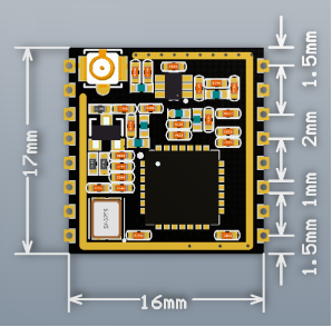
3.1 Dimensions of Ra-01/Ra-02 modules.
3.2 Ra-01/Ra-02 Module Size Comparison Table
| Module model | Length (mm) | Width (mm) | Height (mm) | PAD size (mm) | Pin pitch (mm) | Shielding shell height (mm) | Board thickness (mm) |
| Ra-01 | 17 | 16 | 3.2 ±0.1 | 1x 1 (bottom layer), 1.778 x1.27 (antenna pad bottom layer) | 2 | 2.2±0.1 | 1.0±0.1 |
| Ra-02 | 17 | 16 | 3.2 ±0.1 | 1x 1 (bottom layer) | 2 | 2.2±0.1 | 1.0±0.1 |
3.3 Ra-01/Ra-02 module PCB package drawing
Figure 6 Ra-01/Ra-02 module PCB package diagram
Note: When laying out the board, try to put the module on the side of the board with the antenna facing outward. No components should be placed at or near the bottom of the antenna. The module should be as far away from power components and electromagnetic components as possible, such as thyristors, relays, inductors, buzzers, and horns.
4. Welding temperature
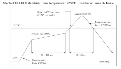
4.1. Reflow soldering temperature
''Note that the temperature should not be too high when soldering the module. The reflow soldering temperature is shown in Table 5:
| Incline heating TS Maximum value -TL | Maximum value 3℃/sec |
| Preheating Minimum temperature value (TS Min.) Typical temperature value (TS Typ.) Maximum temperature value (TS Max .) Time (TS) | 150℃ 175℃ 200℃ 60~180 seconds |
| Inclined heating (TL to TP) | Maximum 3℃/sec |
| Duration/Temperature (TL)/Time (TL) | 217℃/60~150 seconds |
| Peak temperature (TP) | Maximum temperature 260℃, lasting 10 seconds |
| Peak target temperature (TP target value) | 260℃+0/-5℃ |
| Actual peak value (tP) 5°C duration | 20~40 seconds |
| Inclined cooling | Maximum 6℃/sec |
| Time required to adjust to the peak temperature from 25℃ (t) | Maximum 8 minutes |
4.2. Reflow soldering curve graph
5. Instructions for use
The working frequency of Anxinke LoRa series modules (Ra-01/Ra-02) is 433MHz. When using the module, the power supply current must be above 250mA. The module is connected to the MCU through the SPI interface, pay attention to the common ground. …
The connection diagram of Ra-01/Ra-02 module and MCU is shown in the figure below:
Figure 8 Module and MCU connection diagram
For reference procedures and more information, please visit the Anxinke LoRa topic: http://wiki.ai-thinker.com/lora
6. Contact us
(3) WeChat public account
(4) Technical support email: support@aithinker.com


